
555 Timer Frequency and Duty Cycle: Where 1.44/((RA+2RB)C) Comes From
How the 555 comparators and the 1/3 and 2/3 thresholds produce the 0.693 and 1.1 constants, why duty cycle stays above 50%, the diode fix, and picking parts that keep time.
· 10 min read
The 555 timer has been in production since 1972, and its astable formula, f = 1.44 ÷ ((RA + 2RB) × C), is probably copied into more notebooks than any other line in hobby electronics. Few people check where the 1.44 comes from, why the duty cycle refuses to drop below 50%, or why the frequency on the scope is 15% off the calculation. This post builds the formulas up from what happens inside the chip, works through a design with real part values, and lists the practical reasons a 555 drifts. The numbers come from the 555 Timer Calculator, which analyses or designs both astable and monostable circuits.
What the chip actually does
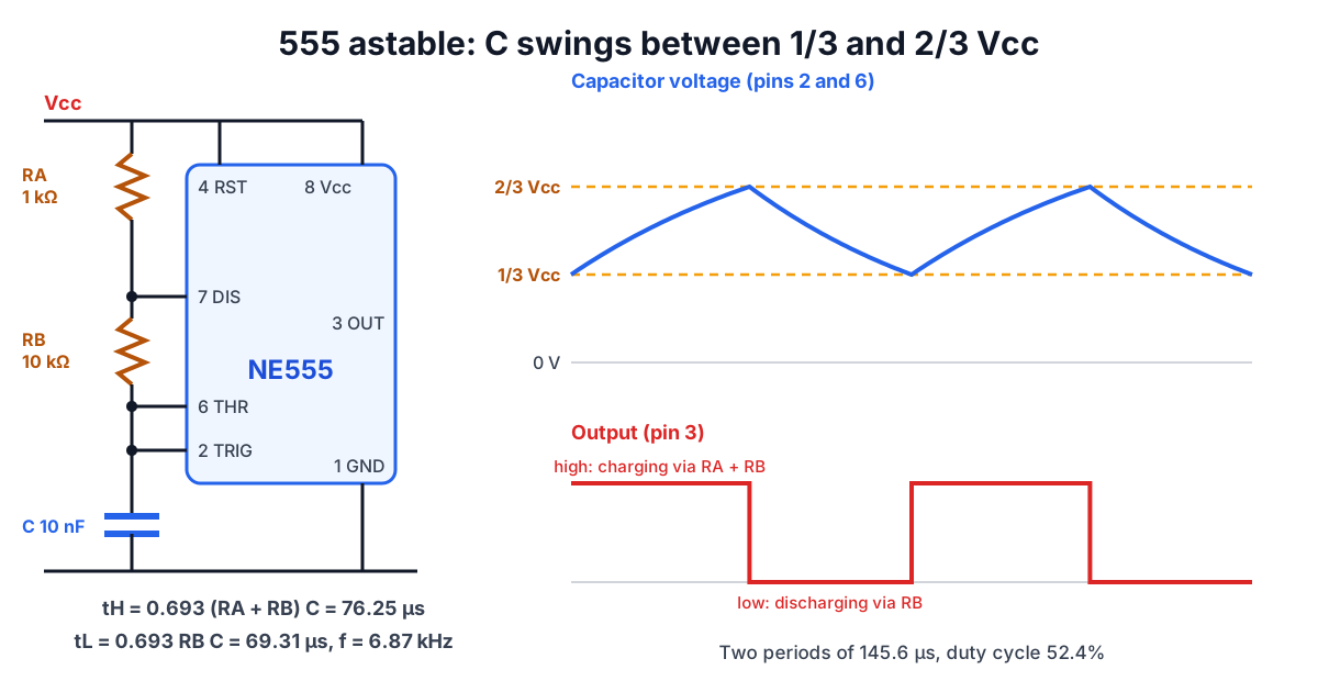
Inside a 555 are three equal resistors forming a divider that sets two reference voltages: 2/3 Vcc and 1/3 Vcc. Two comparators watch the timing capacitor:
- The threshold comparator (pin 6) trips when the capacitor reaches 2/3 Vcc. It resets an internal flip-flop, which drives the output (pin 3) low and turns on the discharge transistor on pin 7.
- The trigger comparator (pin 2) trips when the voltage falls below 1/3 Vcc. It sets the flip-flop, the output goes high and the discharge transistor turns off.
Everything else follows from those two thresholds. In the astable circuit pins 2 and 6 are tied together to the capacitor, so it bounces forever between 1/3 and 2/3 of the supply. Because both thresholds are fractions of Vcc, the timing is in principle independent of the supply voltage, which is one reason the chip became so popular.
Deriving 0.693, 1.44 and 1.1
A capacitor charging through a resistor toward a final voltage Vf follows V(t) = Vf − (Vf − V0) × e^(−t/RC). Charging starts at 1/3 Vcc and heads toward Vcc. Setting V(t) = 2/3 Vcc and solving:
2/3 = 1 − (2/3) × e^(−t/RC), so e^(−t/RC) = 1/2, and t = RC × ln 2 = 0.693 RC
Discharge runs from 2/3 Vcc toward 0 V and stops at 1/3 Vcc, which is again a factor of 2, so it also takes ln 2 time constants. The only difference is the resistance in each path:
- Charging current flows from Vcc through RA and RB into C: tH = 0.693 × (RA + RB) × C
- Discharging current flows from C through RB into pin 7: tL = 0.693 × RB × C
The period is the sum, T = 0.693 × (RA + 2RB) × C, and the frequency is its reciprocal. 1 ÷ 0.693 = 1.4427, which the datasheet rounds to 1.44. The Texas Instruments NE555 datasheet gives exactly these expressions.
The monostable is different because the capacitor starts fully discharged at 0 V and charges to 2/3 Vcc. Solving 2/3 = 1 − e^(−t/RC) gives t = RC × ln 3 = 1.0986 RC, rounded to the familiar 1.1 RC.
Worked example: 1 kΩ, 10 kΩ and 10 nF
With RA = 1 kΩ, RB = 10 kΩ and C = 10 nF:
- tH = 0.693 × 11 kΩ × 10 nF = 76.25 µs
- tL = 0.693 × 10 kΩ × 10 nF = 69.31 µs
- T = 145.6 µs, so f = 6.87 kHz
- Duty cycle = tH ÷ T = 11 ÷ 21 = 52.38%
The rounded 1.44 constant gives 6.857 kHz, a difference of 0.2% that is far smaller than any capacitor tolerance. The calculator uses ln 2 exactly.
Why the duty cycle stays above 50%, and the diode fix
Look at the two paths again. RA appears only in the charging path, so the high time is always longer than the low time. Duty = (RA + RB) ÷ (RA + 2RB), which approaches 50% as RA becomes small compared with RB but never reaches it. You cannot simply set RA to zero: pin 7 would then connect straight to Vcc when the discharge transistor turns on, and the transistor would try to sink the full supply current. Keep RA at 1 kΩ or more.
The standard fix is a diode across RB, anode on pin 7 and cathode toward the capacitor. While charging, current takes the diode and bypasses RB, so tH = 0.693 × RA × C. While discharging, the diode is reverse biased and current flows through RB as before. Now duty = RA ÷ (RA + RB), anything from a few percent to 95% or more, and equal resistors give a near-perfect square wave.
The diode's forward drop of about 0.6 V means the capacitor charges toward Vcc − 0.6 V rather than Vcc, which lengthens tH. On a 12 V supply the effect is a few percent; at 5 V it is closer to 10%. A Schottky diode reduces it.
For a 1 kHz, 25% clock with a 10 nF capacitor the calculator gives RA = 36.07 kΩ and RB = 108.2 kΩ. The nearest E24 parts, 36 kΩ and 110 kΩ, land at 988.1 Hz and 24.7%.
Designing from a target frequency
The design problem has three unknowns and two equations, so one part is a free choice. The usual order is:
- Choose the capacitor first. Capacitors come in coarser steps and wider tolerances than resistors, and their type matters most for stability.
- Solve for RB from the low time: RB = tL ÷ (0.693 × C).
- Solve for RA from the high time: RA = tH ÷ (0.693 × C) − RB (or without subtracting RB in diode mode).
- Check the range. Both resistors should land between about 1 kΩ and 1 MΩ. Below 1 kΩ the discharge transistor works hard; above a few megohms the threshold input current (up to about 250 nA on a bipolar NE555) and the capacitor's leakage start to steal charging current.
- Round to standard values and recalculate. For 1 kHz at 60% with 10 nF, the exact values are 28.85 kΩ and 57.71 kΩ; 30 kΩ and 56 kΩ give 1.016 kHz, 1.6% high.
The calculator's suggested capacitor does step 4 automatically, searching E6 values for the one that keeps both resistors near 47 kΩ, and its table shows the resistor pair for each decade of capacitance so you can see the trade-off.
Why the real frequency is off
When a built 555 misses the calculation, the cause is almost always one of these:
- Capacitor tolerance. Electrolytics are typically ±20%, and class 2 ceramics such as X7R lose capacitance with DC bias. A 10 µF electrolytic flasher can easily be 15% fast or slow. Film and C0G capacitors are the right choice for timing; see Reading Capacitor Codes for what the markings mean.
- Leakage. Electrolytic leakage acts like a resistor across C, slowing the charge toward 2/3 Vcc. With multi-megohm timing resistors it can stop the oscillator altogether.
- Speed limits. The bipolar NE555 has propagation delays of the order of 100 ns. At 100 kHz and above, that is a noticeable slice of the period and the real frequency is lower than calculated. CMOS versions such as the TLC555 and LMC555 run into the megahertz range and draw microamps instead of milliamps.
- Control pin noise. Pin 5 sits on the internal divider. Without a 10 nF capacitor to ground, supply noise moves the thresholds and adds jitter.
- Supply dips. The output stage of a bipolar 555 draws large current spikes at each transition. Decouple pin 8 to pin 1 with 100 nF placed right at the chip.
The monostable in practice
A one-shot needs only R and C. A falling edge on pin 2 below 1/3 Vcc starts the pulse; the output goes high, the discharge transistor releases the capacitor, and the output falls when C reaches 2/3 Vcc after 1.1 RC. With 100 kΩ and 10 µF that is 1.0986 seconds.
Two details catch people. The trigger must return high before the timing ends, or the output stays high; couple a long trigger through a small capacitor so it becomes a short pulse. And the 555 is not retriggerable: a second trigger during the pulse is ignored rather than extending it. For a retriggerable delay, use a dedicated monostable such as the 74HC123.
Related tools and reading
- The 555's timing network is an RC circuit; the same exponential sets the corner of an RC filter. See RC Filter Cutoff Frequency and the RC Filter Calculator.
- Build an odd timing resistor from stock parts with the Series and Parallel Calculator.
- If the 555 drives an LED, size its resistor with the LED Resistor Calculator, remembering that a bipolar 555 output sits up to about 1.7 V below Vcc when sourcing heavy current.
- Check what a capacitor marked 103 or 104 really is with the Capacitor Code Calculator.