
PCB Trace Width for Current: IPC-2221, IPC-2152 and Judgment
Where the IPC-2221 trace equation comes from, why inner layers need 2.6 times the copper, how copper weight and voltage drop change the answer, and when to move to IPC-2152.
· 10 min read

How wide should a PCB trace be for 2 amps? Most designers answer with a calculator, and most calculators answer with one equation from IPC-2221. That equation is useful, but it is a curve fit to charts drawn from tests made decades ago on boards without the copper planes almost every modern board has. This post explains what the equation says, where its numbers come from, how copper weight and layer change the answer, why voltage drop is often the real limit, and when to reach for IPC-2152 instead. The figures come from the PCB Trace Width Calculator.
The problem: heat in a thin conductor
A trace is a resistor. The current I through resistance R produces I²R of heat, and the trace warms until it sheds heat as fast as it is generated, by conduction into the laminate and by convection and radiation from the board surface. The steady temperature rise depends on the cross-section (resistance falls as area grows), the surface available to shed heat (which grows with width), and where the trace sits (surface or buried).
Too much rise has real consequences. FR-4 has a glass transition temperature of around 130 to 170 °C, solder joints weaken at high temperature, nearby components derate, and copper resistance itself climbs 0.39% per °C, which heats the trace further. Designers therefore pick an allowed rise, commonly 10 °C, sometimes 20 to 30 °C for power traces, and size the trace to stay within it.
The IPC-2221 equation
IPC-2221, the generic standard for printed board design, includes a chart of current against cross-section for several temperature rises, derived from older military standard data. Almost every online calculator uses a curve fit to that chart:
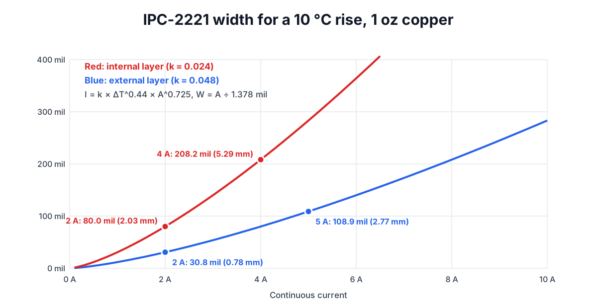
I = k × ΔT^0.44 × A^0.725
where I is the current in amps, ΔT the temperature rise in °C, A the cross-sectional area in square mils, and k = 0.048 for external layers or 0.024 for internal layers. Rearranged for area:
A = (I ÷ (k × ΔT^0.44))^(1/0.725)
Then width = A ÷ thickness. Copper thickness is specified by weight per square foot: 1 oz/ft² is about 1.378 mil (35 µm) thick, so 0.5 oz is 17.5 µm, 2 oz is 70 µm and 3 oz is 105 µm.
Worked example: 2 A at a 10 °C rise
For 2 A on an external layer, 1 oz copper, 10 °C rise:
- k × ΔT^0.44 = 0.048 × 10^0.44 = 0.048 × 2.754 = 0.1322
- A = (2 ÷ 0.1322)^(1/0.725) = 15.13^1.379 = 42.39 mil²
- Width = 42.39 ÷ 1.378 = 30.76 mil, or 0.781 mm
That matches the 31 mil figure quoted by most references. Over 50 mm at 35 °C (25 °C ambient plus the 10 °C rise), the trace resistance is 33.4 mΩ, so it drops 66.7 mV and dissipates 133.5 mW.
What the exponents tell you
The exponents carry most of the practical insight:
- Current goes as A^0.725, not A. Doubling the area raises the allowed current by only 2^0.725 = 1.65 times, because a bigger trace also has relatively less surface per unit of copper. Equivalently, doubling the current needs 2^(1/0.725) = 2.6 times the area.
- Temperature rise matters gently. Current goes as ΔT^0.44, so accepting 20 °C instead of 10 °C allows 36% more current. For 5 A on 1 oz outer copper, width falls from 108.9 mil at 10 °C to 71.5 mil at 20 °C.
- Inner layers need 2.6 times the area. Halving k has the same effect as halving the current capability, so the width scales by 2^(1/0.725). On 1 oz copper at 10 °C, 2 A needs 80.0 mil inside versus 30.8 mil outside.
- Copper weight trades directly against width. Area is what matters, so 2 oz copper halves the width: 2 A at 10 °C needs 15.4 mil on 2 oz outer copper.
Why IPC-2221 is only a starting point
The curves behind the equation cover roughly 0 to 35 A, widths up to 400 mil, 10 to 100 °C rise and 0.5 to 3 oz copper; the calculator warns outside that range rather than extrapolating silently. More importantly, the test boards were simple and had no internal planes, and the internal-layer values are a simple derating of the external ones rather than a separate measurement of buried traces in modern stack-ups.
IPC-2152, published in 2009, replaced this with a much larger set of measurements. Its findings change the picture in two ways:
- Internal traces are usually better than IPC-2221 says. In a modern multilayer board the laminate around an inner trace connects it thermally to planes that spread heat widely. IPC-2152 charts give inner and outer traces similar capacity, and IPC-2221's inner-layer widths are often conservative by a wide margin.
- Board construction dominates. Thickness, the presence and distance of copper planes, and mounting all matter. IPC-2152 provides a baseline chart plus modifiers for these factors.
The practical reading is: IPC-2221 gives a safe, quick width for outer layers and a conservative one for inner layers in most multilayer boards. When currents are high, space is tight, or the board is unusual (thin, flexible, no planes, in still air in a hot enclosure), use the IPC-2152 charts or a thermal simulation, and measure a prototype with a thermal camera.
Voltage drop is often the tighter limit
Temperature is only one constraint. A 3.3 V rail feeding a processor might allow a 1 to 2% drop, about 33 to 66 mV, across the whole path from regulator to load. The resistance of a trace is R = ρ × L ÷ A, with copper's resistivity 1.724 × 10⁻⁸ Ω·m at 20 °C rising 0.393% per °C. A 10 mil, 1 oz trace 100 mm long is about 0.19 Ω, so 1 A drops 0.19 V, already far beyond the budget even though IPC-2221 says the trace would warm by only about 13 °C.
For low-voltage, high-current rails, size for voltage drop first and check temperature second. Short, wide traces, pours and planes are the usual answer, and measuring the voltage at the load (remote sense) helps when the regulator supports it. The same reasoning applies to cable; see How to Size Electrical Wire for the wiring version.
Practical details that move the answer
- Plating adds copper on outer layers. Through-hole plating deposits extra copper on the surface, so "1 oz" outer layers often finish at 1.4 oz or more. Ask your fabricator for the finished thickness.
- Etching narrows traces. The cross-section is a trapezoid slightly narrower at the top, so the effective area is a little below width times thickness. Leave margin on narrow traces.
- Neighbours heat each other. Several power traces side by side, or a trace under a hot regulator, run hotter than an isolated trace.
- Short traces between big pads run cooler. The pads and vias conduct heat away, so the formula is conservative for short connections and accurate for long isolated runs.
- Vias need sizing too. A via's plated barrel is a small tube of copper. Use several vias in parallel on power paths, especially when changing layers.
- Fabricator minimums. Standard processes typically go down to 4 to 6 mil trace and space; very small calculated widths round up to that.
Related tools and reading
- For the cables feeding the board, use the Wire Size Calculator and the Voltage Drop Calculator.
- Check the power in a resistor or trace with the Ohm's Law Calculator.
- LED arrays are a common high-current case; size the per-string resistors with the LED Resistor Calculator and LED Current-Limiting Resistors.